Board Description
More detailed description of LimePSB RPCM board components and interconnections is given in the following sections of this chapter.
Raspberry CM4 Connector
LimePSB RPCM board is designed to use Raspberry Pi CM4 as a host computer. Raspberry Pi CM4L version without eMMC Flash memory is also supported. Board to board connectors (J1 and J2) are used to connect CM4 to the LimePSB RPCM board. Connector pinout, CM4 signals and schematic signal names are listed and described in Table 1.
CM4 Pin |
CM4 reference |
Schematic signal name |
Description[1] |
|---|---|---|---|
1 |
GND |
GND |
Ground (0V) |
2 |
GND |
GND |
Ground (0V) |
3 |
Ethernet_Pair3_P |
ETH_TRD3_P |
Ethernet pair 3 positive |
4 |
Ethernet_Pair1_P |
ETH_TRD1_P |
Ethernet pair 1 positive |
5 |
Ethernet_Pair3_N |
ETH_TRD3_N |
Ethernet pair 3 negative |
6 |
Ethernet_Pair1_N |
ETH_TRD1_N |
Ethernet pair 1 negative |
7 |
GND |
GND |
Ground (0V) |
8 |
GND |
GND |
Ground (0V) |
9 |
Ethernet_Pair2_N |
ETH_TRD2_N |
Ethernet pair 2 negative |
10 |
Ethernet_Pair0_N |
ETH_TRD0_N |
Ethernet pair 0 negative |
11 |
Ethernet_Pair2_P |
ETH_TRD2_P |
Ethernet pair 2 positive |
12 |
Ethernet_Pair0_P |
ETH_TRD0_P |
Ethernet pair 0 positive |
13 |
GND |
GND |
Ground (0V) |
14 |
GND |
GND |
Ground (0V) |
15 |
Ethernet_nLED3 |
ETH_LED_Y |
Ethernet activity indicator |
16 |
Ethernet_SYNC_IN |
RPI_SYNC_IN_LS |
IEEE1588 SYNC Input |
17 |
Ethernet_nLED2 |
ETH_LED_G |
Ethernet speed indicator |
18 |
Ethernet_SYNC_OUT |
RPI_SYNC_OUT_LS |
IEEE1588 SYNC Output |
19 |
Ethernet_nLED1 |
NC |
Ethernet speed indicator |
20 |
EEPROM_nWP |
RPI_EEPROM_nWP |
EEPROM write protect |
21 |
Pi_nLED_Activity |
RPI_STATUS_LED_G |
Pi activity LED |
22 |
GND |
GND |
Ground (0V) |
23 |
GND |
GND |
Ground (0V) |
24 |
GPIO26 |
PCIE_LED_WPAN |
General purpose |
25 |
GPIO21 |
RPI_SPI1_SCLK |
General purpose |
26 |
GPIO19 |
RPI_SPI1_MISO |
General purpose |
27 |
GPIO20 |
RPI_SPI1_MOSI |
General purpose |
28 |
GPIO13 |
RPI_PWM1 |
General purpose |
29 |
GPIO16 |
PCIE_LED_WWAN |
General purpose |
30 |
GPIO6 |
RPI_RF_SW_TDD |
General purpose |
31 |
GPIO12 |
RPI_PWM0 |
General purpose |
32 |
GND |
GND |
Ground (0V) |
33 |
GND |
GND |
Ground (0V) |
34 |
GPIO5 |
BUZZER |
General purpose |
35 |
ID_SC |
RPI_ID_SC |
BCM2711 GPIO 1 |
36 |
ID_SD |
RPI_ID_SD |
BCM2711 GPIO 0 |
37 |
GPIO7 |
RPI_SPI0_SS1 |
General purpose |
38 |
GPIO11 |
RPI_SPI0_SCLK |
General purpose |
39 |
GPIO8 |
RPI_SPI0_SS0 |
General purpose |
40 |
GPIO9 |
RPI_SPI0_MISO |
General purpose |
41 |
GPIO25 |
PCIE_LED_WLAN |
General purpose |
42 |
GND |
GND |
Ground (0V) |
43 |
GND |
GND |
Ground (0V) |
44 |
GPIO10 |
RPI_SPI0_MOSI |
General purpose |
45 |
GPIO24 |
RPI_BTN1 |
General purpose |
46 |
GPIO22 |
RPI_GPIO22 |
General purpose |
47 |
GPIO23 |
RPI_BTN2 |
General purpose |
48 |
GPIO27 |
RPI_GPIO27 |
General purpose |
49 |
GPIO18 |
RPI_SPI1_SS0 |
General purpose |
50 |
GPIO17 |
RPI_SPI1_SS1 |
General purpose |
51 |
GPIO15 |
RPI_UART0_RX |
General purpose |
52 |
GND |
GND |
Ground (0V) |
53 |
GND |
GND |
Ground (0V) |
54 |
GPIO4 |
RPI_GPIO4 |
General purpose |
55 |
GPIO14 |
RPI_UART0_TX |
General purpose |
56 |
GPIO3 |
ADF_MUXOUT |
General purpose |
57 |
SD_CLK |
RPI_SD_CLK |
SD card clock signal |
58 |
GPIO2 |
RPI_GPIO2 |
General purpose |
59 |
GND |
GND |
Ground (0V) |
60 |
GND |
GND |
Ground (0V) |
61 |
SD_DAT3 |
RPI_SD_D3 |
SD card/eMMC Data3 signal |
62 |
SD_CMD |
RPI_SD_CMD |
SD card/eMMC Command signal |
63 |
SD_DAT0 |
RPI_SD_D0 |
SD card/eMMC Data0 signal |
64 |
SD_DAT5 |
NC |
SD card/eMMC Data5 signal |
65 |
GND |
GND |
Ground (0V) |
66 |
GND |
GND |
Ground (0V) |
67 |
SD_DAT1 |
RPI_SD_D1 |
SD card/eMMC Data1 signal |
68 |
SD_DAT4 |
NC |
SD card/eMMC Data4 signal |
69 |
SD_DAT2 |
RPI_SD_D2 |
SD card/eMMC Data2 signal |
70 |
SD_DAT7 |
NC |
SD card/eMMC Data7 signal |
71 |
GND |
GND |
Ground (0V) |
72 |
SD_DAT6 |
NC |
SD card/eMMC Data6 signal |
73 |
SD_VDD_Override |
NC |
Force SD card/eMMC interface |
74 |
GND |
GND |
Ground (0V) |
75 |
SD_PWR_ON |
RPI_SD_PWR_ON |
Output to power-switch for the SD card |
76 |
Reserved |
NC |
Do not connect |
77 |
+5V (Input) |
VCC5P0 |
4.75V-5.25V. Main power input |
78 |
GPIO_VREF |
VCC3P3 |
GPIO reference voltage |
79 |
+5V (Input) |
VCC5P0 |
4.75V-5.25V. Main power input |
80 |
SCL0 |
RPI_I2C0_SCL |
I2C clock pin |
81 |
+5V (Input) |
VCC5P0 |
4.75V-5.25V. Main power input |
82 |
SDA0 |
RPI_I2C0_SDA |
I2C Data pin |
83 |
+5V (Input) |
VCC5P0 |
4.75V-5.25V. Main power input |
84 |
CM4_3.3V (Output) |
VCC3P3_RPI |
3.3V ± 2.5%. Power Output |
85 |
+5V (Input) |
VCC5P0 |
4.75V-5.25V. Main power input |
86 |
CM4_3.3V (Output) |
VCC3P3_RPI |
3.3V ± 2.5%. Power Output |
87 |
+5V (Input) |
VCC5P0 |
4.75V-5.25V. Main power input |
88 |
CM4_1.8V (Output) |
VCC1P8_RPI |
1.8V ± 2.5%. Power Output |
89 |
WL_nDisable |
RPI_WL_nDISABLE |
Wireless interface disable |
90 |
CM4_1.8V (Output) |
VCC1P8_RPI |
1.8V ± 2.5%. Power Output |
91 |
BT_nDisable |
RPI_BT_nDISABLE |
Bluetooth interface disable |
92 |
RUN_PG |
RPI_RUN_PG |
CM4 CPU reset/power good |
93 |
nRPIBOOT |
RPI_nRPIBOOT |
booting from an RPI server |
94 |
AnalogIP1 |
RPI_AIP1 |
Analogue input |
95 |
PI_LED_nPWR |
RPI_LED_nPWR |
Power On LED |
96 |
AnalogIP0 |
RPI_AIP0 |
Analogue input |
97 |
Camera_GPIO |
CAM1_GPIO0 |
Used to shut down the camera |
98 |
GND |
GND |
Ground (0V) |
99 |
GLOBAL_EN |
RPI_GLOBAL_EN |
CM4 enable |
100 |
nEXTRST |
RPI_nEXTRST |
Output. Driven low during reset |
101 |
USB_OTG_ID |
RPI_USB_OTG_ID |
USB OTG Pin |
102 |
PCIe_CLK_nREQ |
RPI_PCIE_CLK_nREQ |
PCIe clock request |
103 |
USB_N |
RPI_USB_D_N |
USB D- |
104 |
Reserved |
NC |
Do not connect |
105 |
USB_P |
RPI_USB_D_P |
USB D+ |
106 |
Reserved |
NC |
Do not connect |
107 |
GND |
GND |
Ground (0V) |
108 |
GND |
GND |
Ground (0V) |
109 |
PCIe_nRST |
RPI_PCIE_nRST |
PCIe reset |
110 |
PCIe_CLK_P |
RPI_PCIE_CLK_P |
PCIe clock Out positive |
111 |
VDAC_COMP |
RPI_TVDAC |
Video DAC output |
112 |
PCIe_CLK_N |
RPI_PCIE_CLK_N |
PCIe clock Out negative |
113 |
GND |
GND |
Ground (0V) |
114 |
GND |
GND |
Ground (0V) |
115 |
CAM1_D0_N |
CAM1_D0_N |
Input Camera1 D0 negative |
116 |
PCIe_RX_P |
RPI_PCIE_RX_P |
Input PCIe GEN 2 RX positive |
117 |
CAM1_D0_P |
CAM1_D0_P |
Input Camera1 D0 positive |
118 |
PCIe_RX_N |
RPI_PCIE_RX_N |
Input PCIe GEN 2 RX negative |
119 |
GND |
GND |
Ground (0V) |
120 |
GND |
GND |
Ground (0V) |
121 |
CAM1_D1_N |
CAM1_D1_N |
Input Camera1 D1 negative |
122 |
PCIe_TX_P |
RPI_PCIE_TX_P |
Output PCIe GEN 2 TX positive |
123 |
CAM1_D1_P |
CAM1_D1_P |
Input Camera1 D1 positive |
124 |
PCIe_TX_N |
RPI_PCIE_TX_N |
Output PCIe GEN 2 TX positive |
125 |
GND |
GND |
Ground (0V) |
126 |
GND |
GND |
Ground (0V) |
127 |
CAM1_C_N |
CAM1_CLK_N |
Input Camera1 clock negative |
128 |
CAM0_D0_N |
NC |
Input Camera0 D0 negative |
129 |
CAM1_C_P |
CAM1_CLK_P |
Input Camera1 clock positive |
130 |
CAM0_D0_P |
NC |
Input Camera0 D0 positive |
131 |
GND |
GND |
Ground (0V) |
132 |
GND |
GND |
Ground (0V) |
133 |
CAM1_D2_N |
NC |
Input Camera1 D2 negative |
134 |
CAM0_D1_N |
NC |
Input Camera0 D1 negative |
135 |
CAM1_D2_P |
NC |
Input Camera1 D2 positive |
136 |
CAM0_D1_P |
NC |
Input Camera0 D1 positive |
137 |
GND |
GND |
Ground (0V) |
138 |
GND |
GND |
Ground (0V) |
139 |
CAM1_D3_N |
NC |
Input Camera1 D3 negative |
140 |
CAM0_C_N |
NC |
Input Camera0 clock negative |
141 |
CAM1_D3_P |
NC |
Input Camera1 D3 positive |
142 |
CAM0_C_P |
NC |
Input Camera0 clock positive |
143 |
HDMI1_HOTPLUG |
HDMI1_HOTPLUG |
Input HDMI1 hotplug |
144 |
GND |
GND |
Ground (0V) |
145 |
HDMI1_SDA |
HDMI1_SDA |
A Bidirectional HDMI1 SDA |
146 |
HDMI1_TX2_P |
HDMI1_D2_P |
Output HDMI1 TX2 positive |
147 |
HDMI1_SCL |
HDMI1_SCL |
Bidirectional HDMI1 SCL |
148 |
HDMI1_TX2_N |
HDMI1_D2_N |
Output HDMI1 TX2 negative |
149 |
HDMI1_CEC |
HDMI1_CEC |
Input HDMI1 CEC |
150 |
GND |
GND |
Ground (0V) |
151 |
HDMI0_CEC |
HDMI0_CEC |
Input HDMI0 CEC |
152 |
HDMI1_TX1_P |
HDMI1_D1_P |
Output HDMI1 TX1 positive |
153 |
HDMI0_HOTPLUG |
HDMI0_HOTPLUG |
Input HDMI0 hotplug |
154 |
HDMI1_TX1_N |
HDMI1_D1_N |
Output HDMI1 TX1 negative |
155 |
GND |
GND |
Ground (0V) |
156 |
GND |
GND |
Ground (0V) |
157 |
DSI0_D0_N |
NC |
Output Display0 D0 negative |
158 |
HDMI1_TX0_P |
HDMI1_D0_P |
Output HDMI1 TX0 positive |
159 |
DSI0_D0_P |
NC |
Output Display0 D0 positive |
160 |
HDMI1_TX0_N |
HDMI1_D0_N |
Output HDMI1 TX0 negative |
161 |
GND |
GND |
Ground (0V) |
162 |
GND |
GND |
Ground (0V) |
163 |
DSI0_D1_N |
NC |
Output Display0 D1 negative |
164 |
HDMI1_CLK_P |
HDMI1_CLK_P |
Output HDMI1 clock positive |
165 |
DSI0_D1_P |
NC |
Output Display0 D1 positive |
166 |
HDMI1_CLK_N |
HDMI1_CLK_N |
Output HDMI1 clock negative |
167 |
GND |
GND |
Ground (0V) |
168 |
GND |
GND |
Ground (0V) |
169 |
DSI0_C_N |
NC |
Output Display0 clock negative |
170 |
HDMI0_TX2_P |
HDMI0_D2_P |
Output HDMI0 TX2 positive |
171 |
DSI0_C_P |
NC |
Output Display0 clock positive |
172 |
HDMI0_TX2_N |
HDMI0_D2_N |
Output HDMI0 TX2 negative |
173 |
GND |
GND |
Ground (0V) |
174 |
GND |
GND |
Ground (0V) |
175 |
DSI1_D0_N |
DSI1_D0_N |
Output Display1 D0 negative |
176 |
HDMI0_TX1_P |
HDMI0_D1_P |
Output HDMI0 TX1 positive |
177 |
DSI1_D0_P |
DSI1_D0_P |
Output Display1 D0 positive |
178 |
HDMI0_TX1_N |
HDMI0_D1_N |
Output HDMI0 TX1 negative |
179 |
GND |
GND |
Ground (0V) |
180 |
GND |
GND |
Ground (0V) |
181 |
DSI1_D1_N |
DSI1_D1_N |
Output Display1 D1 negative |
182 |
HDMI0_TX0_P |
HDMI0_D0_P |
Output HDMI0 TX0 positive |
183 |
DSI1_D1_P |
DSI1_D1_P |
Output Display1 D1 positive |
184 |
HDMI0_TX0_N |
HDMI0_D0_N |
Output HDMI0 TX0 negative |
185 |
GND |
GND |
Ground (0V) |
186 |
GND |
GND |
Ground (0V) |
187 |
DSI1_C_N |
DSI1_CLK_N |
Output Display1 clock negative |
188 |
HDMI0_CLK_P |
HDMI0_CLK_P |
Output HDMI0 clock positive |
189 |
DSI1_C_P |
DSI1_CLK_P |
Output Display1 clock positive |
190 |
HDMI0_CLK_N |
HDMI0_CLK_N |
Output HDMI0 clock negative |
191 |
GND |
GND |
Ground (0V) |
192 |
GND |
GND |
Ground (0V) |
193 |
DSI1_D2_N |
NC |
Output Display1 D2 negative |
194 |
DSI1_D3_N |
NC |
Output Display1 D3 negative |
195 |
DSI1_D2_P |
NC |
Output Display1 D2 positive |
196 |
DSI1_D3_P |
NC |
Output Display1 D3 positive |
197 |
GND |
GND |
Ground (0V) |
198 |
GND |
GND |
Ground (0V) |
199 |
HDMI0_SDA |
HDMI0_SDA |
Bidirectional HDMI0 SDA |
200 |
HDMI0_SCL |
HDMI0_SCL |
Bidirectional HDMI0 SCL |
Raspberry Pi CM4 Configuration Headers
LimePSB RPCM board has several headers dedicated for Raspberry Pi CM4 configuration, debug, analog inputs or other purposes. Header J14 (SYS) pins, schematic signal names and description are given in Table 2.
Pin |
Schematic signal name |
Description |
|---|---|---|
1 |
GND |
Ground (0V) |
2 |
RPI_nRPIBOOT |
A low on this pin forces CM4 booting. To enable Raspberry Pi USB boot also place nRPIBOOT jumper on J14 pins 1-2. Place jumper on header J28 to switch Raspberry Pi USB from USB hub to USB C connector. |
3 |
GND |
Ground (0V) |
4 |
RPI_EEPROM_nWP |
CM4 on-board EEPROM write protect |
5 |
RPI_AIP0 |
Analogue input |
6 |
RPI_AIP1 |
Analogue input |
7 |
GND |
Ground (0V) |
8 |
RPI_SYNC_IN |
IEEE1588 SYNC Input |
9 |
RPI_SYNC_OUT |
IEEE1588 SYNC Output |
10 |
GND |
Ground (0V) |
11 |
RPI_TVDAC |
Video DAC output |
12 |
GND |
Ground (0V) |
13 |
RPI_RUN_PG_BUFF |
Buffered (5V output) RPI_RUN_PG line. High signal indicates CM4 CPU is running. |
14 |
RPI_GLOBAL_EN |
Drive low to power off CM4. A button between pins 13-14 can be used to wake up compute module from power down. |
Description of additional control connector J5 (not fitted) for Raspberry Pi CM4 pinout is given in Table 3.
Pin |
Schematic signal name |
Description |
|---|---|---|
1 |
RPI_GLOBAL_EN |
Drive low to power off CM4. |
2 |
GND |
Ground (0V) |
3 |
RPI_RUN_PG |
Drive low to reset CM4 CPU/high signal indicates CM4 CPU is running. |
Raspberry Pi Compute Module 4 on board WiFi and Bluetooth disable signals may be controlled by header J6 (not fitted) as shown in Table 4.
Pin |
Schematic signal name |
Description |
|---|---|---|
1 |
RPI_WL_nDISABLE |
Drive low to disable wireless interface |
2 |
GND |
Ground (0V) |
3 |
RPI_BT_nDISABLE |
Drive low to reset CM4 CPU/high signal indicates CM4 CPU is running |
Mini PCIe x1 Socket
LimePSB RPCM board features mini PCIe x1 specification compatible socket. LimePSB RPCM board mPCIe socket is also compatible with some non-standard expansion boards like LimeSDR XTRX, LoRaWAN and LoRa Core. More detailed information is listed in Table 5.
Pin |
Mini PCIe x1 Specification Reference |
LimePSB RPCM schematic signal name |
XTRX reference |
LoRaWAN reference |
SX1302/03 Corecell schematic signal name |
|---|---|---|---|---|---|
1 |
Wake# |
NC |
Wake# |
NC |
NC |
2 |
3.3 Vaux |
VCC3P3 |
+3.3V |
VCC |
VCC5V_IN |
3 |
COEX1 |
PCIE_COEX1 |
1PPSI_GPIO1(1N) |
NC |
NC |
4 |
GND |
GND |
GND |
GND |
GND |
5 |
COEX2 |
PCIE_COEX2 |
1PPSO_GPIO2(1P) |
PPS_IN |
NC |
6 |
GND |
VCC1P5 |
+1.5V |
NC |
GPIO(6) (NC) |
7 |
CLKREQ# |
RPI_PCIE_CLK_nREQ |
CLKREQ# |
NC |
NC |
8 |
UIM PWR |
UIM_PWR |
UIM_PWR |
NC |
NC |
9 |
GND |
GND |
GND |
GND |
GND |
10 |
UIM_DATA |
UIM_DATA |
UIM_DATA |
SWDIO |
NC |
11 |
REFCLK- |
RPI_PCIE_CLK_N |
REF_CLK- |
NC |
NC |
12 |
UIM_CLK |
UIM_CLK |
UIM_CLK |
SWCLK |
NC |
13 |
REFCLK+ |
RPI_PCIE_CLK_P |
REF_CLK+ |
NC |
NC |
14 |
UIM_RESET |
UIM_RESET |
UIM_RESET |
NC |
NC |
15 |
GND |
GND |
GND |
GND |
GND |
16 |
UIM_VPP |
UIM_VPP |
UIM_VPP |
BOOT0 |
POWER_EN(NC) |
17 |
Reserved |
PCIE_UIM8 |
TDD_GPIO3_N |
NC |
HOST_SCK (NC) |
18 |
GND |
GND |
GND |
GND |
GND |
19 |
Reserved |
PCIE_UIMC4 |
MHZ_IN |
NC |
HOST_MISO(NC) |
20 |
W_DISABLE# |
NC |
TDD_GPIO3_P |
nDISABLE |
NC |
21 |
GND |
GND |
GND |
GND |
GND |
22 |
PERST# |
RPI_PCIE_nRST |
PERST# |
nRESET |
SX1302_RESET_HOST (NC) |
23 |
PERn0 |
RPI_PCIE_RX_N |
PERn0 |
NC |
HOST_MOSI(NC) |
24 |
3.3Vaux |
VCC3P3 |
+3.3Vaux |
VCC |
SX1261_BUSY (NC) |
25 |
PERp0 |
RPI_PCIE_RX_P |
PERp0 |
NC |
HOST_CSN (NC) |
26 |
GND |
GND |
GND |
GND |
GND |
27 |
GND |
GND |
GND |
GND |
GND |
28 |
1.5Volt |
VCC1P5 |
+1.5V |
NC |
SX1302_GPIO_8 (NC) |
29 |
GND |
GND |
GND |
GND |
GND |
30 |
SMB CLK |
PCIE_SMB_CLK |
MHZ_OUT |
NC |
I2C_SCL (NC) |
31 |
PETn0 |
PCIE_PET0_N |
PETn0 |
NC |
PPS |
32 |
SMB Data |
PCIE_SMB_DATA |
GPIO8 |
NC |
I2C_SDA (NC) |
33 |
PETp0 |
PCIE_PET0_P |
PETp0 |
NC |
NC |
34 |
GND |
GND |
GND |
GND |
GND |
35 |
GND |
GND |
GND |
GND |
GND |
36 |
USB_D- |
PCIE_USB_N |
USB_DN |
USB_D- / Tx |
USB_DM |
37 |
GND |
GND |
GND |
GND |
GND |
38 |
USB_D+ |
PCIE_USB_P |
USB_DP |
USB_D+ / Rx |
USB_DP |
39 |
3.3Vaux |
VCC3P3 |
PERp1 |
VCC |
VCC3V3_IN |
40 |
GND |
GND |
GND |
GND |
GND |
41 |
3.3Vaux |
VCC3P3 |
PERp1 |
VCC |
VCC3V3_IN |
42 |
LED_WWAN# |
PCIE_LED_WWAN |
LED_WWAN#_GPIO5 |
nTX |
NC |
43 |
GND |
GND |
GND |
GND |
GND |
44 |
LED_WLAN# |
PCIE_LED_WLAN |
LED_WLAN#_GPIO6 |
nRX |
SX1261_NSS (NC) |
45 |
Reserved |
NC |
GND |
NC |
JTCK-SWCLK (NC) |
46 |
LED_WPAN# |
PCIE_LED_WPAN |
LED_WPAN#_GPIO7 |
NC |
SX1261_DIO1 (NC) |
47 |
Reserved |
NC |
PETn1 |
NC |
JTMS-SWDIO (NC) |
48 |
1.5Volt |
VCC1P5 |
+1.5V |
NC |
SX1261_NRESET(NC) |
49 |
Reserved |
NC |
PETp1 |
NC |
MCU_NRESET (NC) |
50 |
GND |
GND |
GND |
GND |
GND |
51 |
Reserved |
NC |
GND |
NC |
MCU_BOOT0 (NC) |
52 |
3.3Vaux |
VCC3P3 |
+3.3V |
VCC |
VCC3V3_IN |
RF Front End
LimePSB RPCM RF path features power amplifiers, low noise amplifiers and SPDT switches as shown in Figure 1.
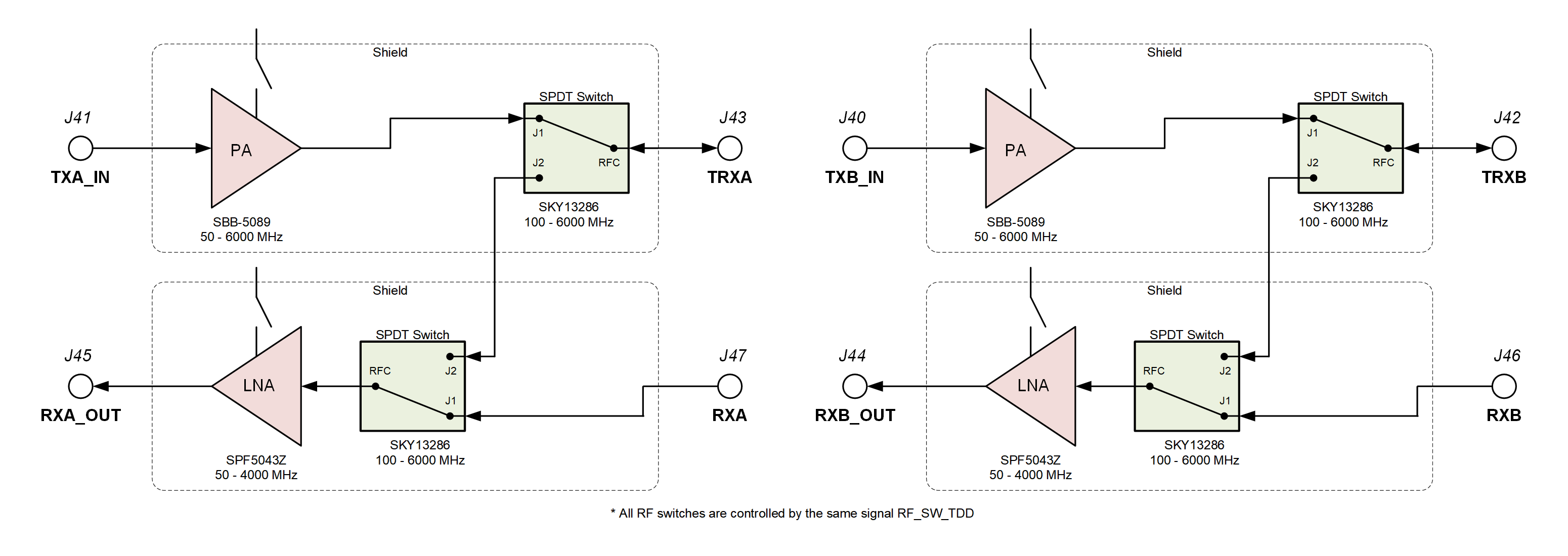
Figure 1: LimePSB RPCM 1v1 RF path block diagram
A single control signal (RF_SW_TDD) is used to control all RF switches simultaneously for both A and B channels to change between TDD and FDD modes as shown in Table 6.
Control signal (RF_SW_TDD) |
TRXA/B connected to |
RXA/B connected to |
|---|---|---|
Low |
TXA/B_IN |
RXA/B_OUT |
High |
RXA/B_OUT |
NC |
By default RF switches may be controlled from mPCIe expansion board pin 17 (via resistor R40). Optional control source may be RFFE TDD control header (J21) or CM4 GPIO6 (resistor R41 must be soldered).
RF path contains two types of connectors: board edge SMA connectors (J42, J43, J46, J47) used for external connections (antennas or cables) and U.FL connectors (J40, J41, J44, J45) used for internal connections (for example to connect to XTRX mini PCIe expansion board).
Signal frequency range of TX and RX paths are listed in Table 7.
Direction |
Frequency range |
|---|---|
TX |
100 MHz - 6 GHz |
RX |
100 MHz - 4 GHz |
More detailed RF path component parameters are given in Table 8.
Component |
Function |
Gain, dB |
Output P1dB, dBm |
NF, dB |
|---|---|---|---|---|
SBB-5089 |
TX amplifier |
20.5dB (850 MHz) 19.0dB (1950 MHz) 15.5dB (6000 MHz) |
20.5dBm (850 MHz) 20.4dBm (1950 MHz) 14.7dBm (4000 MHz) |
3.8dB (850 MHz) 4.1dB (1950 MHz) 4.6dB (4000 MHz) |
SPF5043Z |
RX amplifier |
18.2dB (900 MHz) 12.9dB (1960 MHz) 7.0dB (3800 MHz) |
22.6dBm (900 MHz) 22.7dBm (1900 MHz) 22.8dBm (3800 MHz) |
0.8dB (900 MHz) 0.8dB (1900 MHz) 1.5dB (3800 MHz) |
SKY13286 |
RF switch |
-0.7dB (1000 MHz) -0.8dB (2000 MHz) -1.6dB (6000 MHz) |
30.dBm (2000 MHz) |
LimePSB RPCM RF front end uses same design as Front End Adapter. For more information about the design check LimeSDR XTRX documentation
USB Subsystem
LimePSB RPCM features USB2.0 hub, type-C, double type-A sockets and headers. The USB subsystem diagram is as shown in Figure 9.
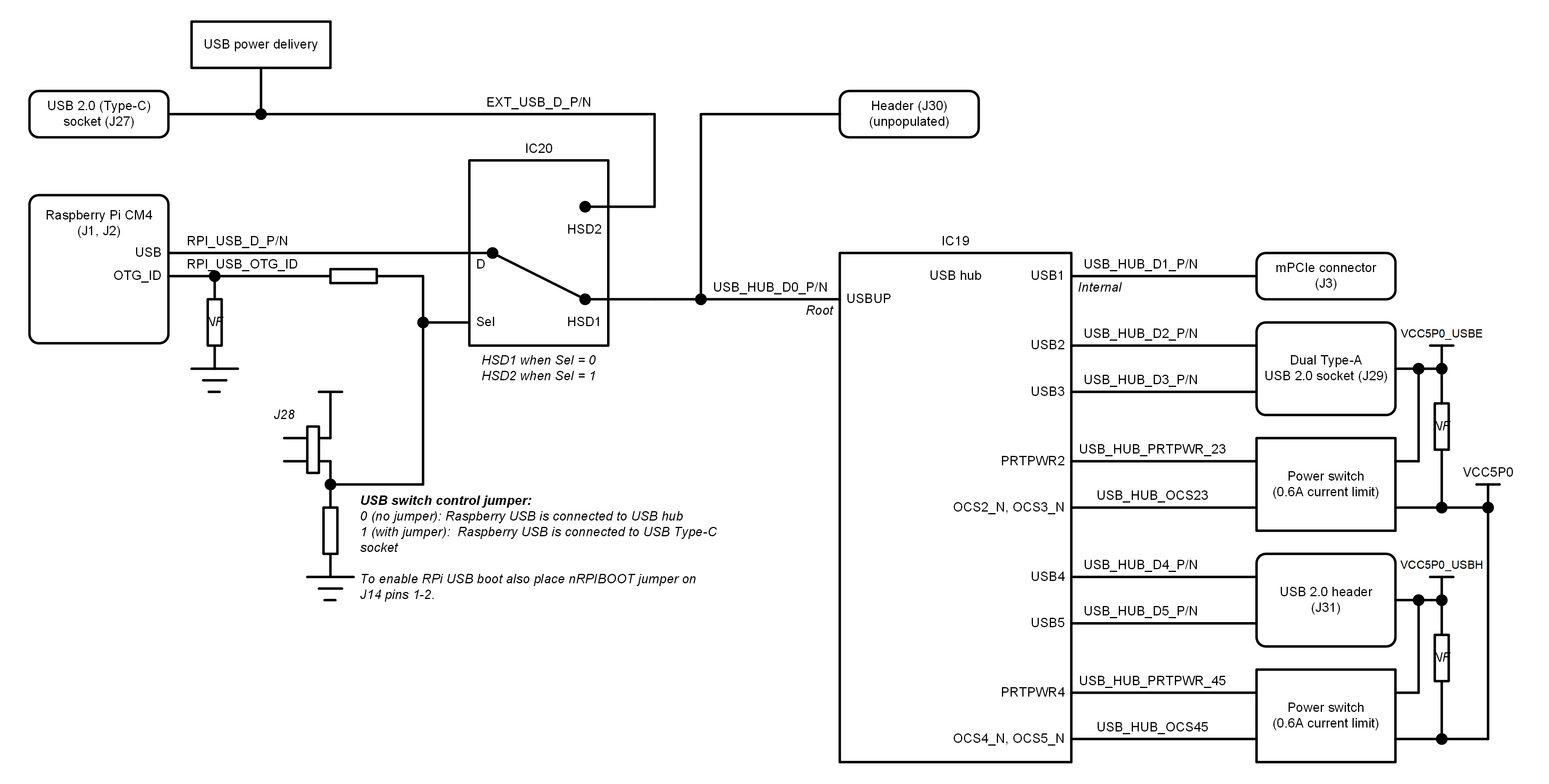
Figure 9. LimePSB RPCM 1v1 USB subsystem diagram
Main LimeSPB RPCM board USB subsystem components:
USB type-C socket (J27) is primarily used as LimeSPB RPCM one of power supply sources (for more information check Power Distribution section). To enable RPi USB boot mount nRPIBOOT jumper on J14 pins 1-2 and mount a jumper on header J28 to switch Raspberry Pi USB from USB hub to USB C (more information check section 2.2 Raspberry Pi CM4 Configuration Headers).
USB type-A dual sockets (J29) may be used to connect USB peripherals to the Raspberry Pi CM4.
USB2.0 hub USB2517 (IC19) USB 2.0 hub expands Raspberry Pi CM4 USB port to dual USB socket (J29), header (J31) and mPCIe (J3). For more information check Table 9.
Pin |
Pin name |
Function |
Schematic signal name |
Connector ID |
|---|---|---|---|---|
59/58 |
USBUP_DP/ USBUP_DM |
Root port |
USB_HUB_D0_P/ USB_HUB_D0_N |
Connected to CM4 USB via USB switch |
2/1 |
USBDN1_DP/ USBDN1_DM |
Downstream port |
USB_HUB_D1_P/ USB_HUB_D1_N |
J3 (mPCIe) |
4/3 |
USBDN2_DP/ USBDN2_DM |
Downstream port |
USB_HUB_D2_P/ USB_HUB_D2_N |
J29 (bottom) |
7/6 |
USBDN3_DP/ USBDN3_DM |
Downstream port |
USB_HUB_D3_P/ USB_HUB_D3_N |
J29 (top)) |
9/8 |
USBDN4_DP/ USBDN4_DM |
Downstream port |
USB_HUB_D4_P/ USB_HUB_D4_N |
J31 (pins 5/3) |
12/11 |
USBDN5_DP/ USBDN5_DM |
Downstream port |
USB_HUB_D5_P/ USB_HUB_D5_N |
J31 (pins 6/4) |
54/53 |
USBDN6_DP/ USBDN6_DM |
Downstream port |
NC |
NC |
56/55 |
USBDN7_DP/ USBDN7_DM |
Downstream port |
NC |
NC |
User Interface Components
LimePSB RPCM board features five dual colour (red and green (RG)) LEDs, one green indication LED and two Ethernet activity LEDs (yellow and green). All board LEDs are highlighted in Figure 2.
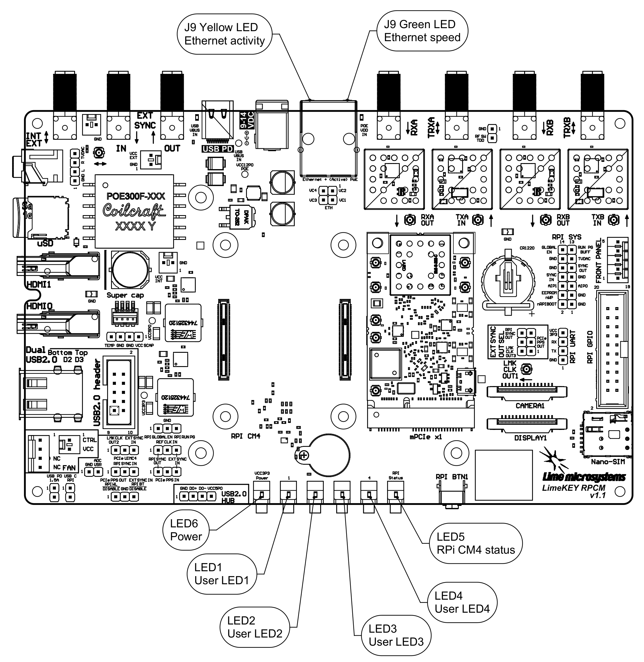
Figure 2: LimePSB RPCM 1v1 user interface components
Dual color LEDs (LED1-LED4) are connected to shift register (IC14). Their function may be programmed according to the user requirements. Dual color LED5 indicates Raspberry Pi status. Green LED6 indicates board power. These LEDs are mounted on the front side of the board.
Ethernet connector J9 has two LEDs: yellow and green. LEDs indicate wired network activity and speed.
Default function of LEDs and related information is listed in Table 10.
Board Reference |
Schematic name |
Shift register (IC14) pin |
Description |
|---|---|---|---|
LED1 |
RPI_LED1_R |
Q0 |
User defined. |
RPI_LED1_G |
Q1 |
||
LED2 |
RPI_LED2_R |
Q2 |
User defined. |
RPI_LED2_G |
Q3 |
||
LED3 |
RPI_LED3_R |
Q4 |
User defined. |
RPI_LED3_G |
Q5 |
||
LED4 |
RPI_LED4_R |
Q6 |
User defined. |
RPI_LED4_G |
Q7 |
||
LED5 |
RPI_STATUS_LED_R |
Green is connected to CM4 PI_LED_nPWR (Power On) and red is connected to Pi_nLED_Activity (Activity). |
|
RPI_STATUS_LED_G |
|||
LED6 |
VCC3P3 |
Board power. Connected to 3.3 V power rail |
|
Ethernet connector J9 LEDs |
ETH_LED_Y |
Green is connected to Ethernet_nLED2 (Ethernet speed indicator: 1Gbit or 100Mbit Link) and yellow is connected to Ethernet_nLED3 (Ethernet activity indicator). |
|
ETH_LED_G |
A user button BTN1 is mounted on the front side of the board and can be used for various purposes. The button is connected to Raspberry Pi CM4 GPIO24, has external pull up resistors and is hardware debounced.
SPI, I2C, UART Interfaces
LimePSB RPCM features multiple low speed interfaces like SPI (SPI0, SPI1), I2C, UART. LimePSB RPCM low speed interfaces signal names, I/O standards are listed in Table 11.
Interface |
Schematic signal name |
CM4 pin |
I/O standard |
Comment |
|---|---|---|---|---|
SPI0 |
RPI_SPI0_SCLK |
38 (GPIO11) |
3.3V |
Serial Clock (CM4 output) |
RPI_SPI0_MOSI |
44 (GPIO10) |
3.3V |
Data (CM4 output) |
|
RPI_SPI0_MISO |
40 (GPIO9) |
3.3V |
Data (CM4 input) |
|
RPI_SPI0_SS0 |
39 (GPIO8) |
3.3V |
IC27 and IC29 DACs SPI slave select (CM4 output) |
|
RPI_SPI0_SS1 |
37 (GPIO7) |
3.3V |
IC28 phase detector SPI slave select (CM4 output) |
|
SPI1 |
RPI_SPI1_SCLK |
25 (GPIO21) |
3.3V |
Serial Clock (CM4 output) |
RPI_SPI1_MOSI |
27 (GPIO20) |
3.3V |
Data (CM4 output) |
|
RPI_SPI1_MISO |
26 (GPIO19) |
3.3V |
Data (CM4 input) |
|
RPI_SPI1_SS0 |
49 (GPIO18) |
3.3V |
IC8 ADC SPI slave select (CM4 output) |
|
RPI_SPI1_SS1 |
50 (GPIO17) |
3.3V |
IC14 AND IC16 Shift registers SPI slave select (CM4 output) |
|
I2C0 |
RPI_I2C0_SCL |
80 |
3.3V |
Serial Clock (CM4 output) |
RPI_I2C0_SDA |
82 |
3.3V |
Data |
|
UART0 |
RPI_UART0_RX |
51 (GPIO15) |
3.3V |
Data (CM4 input) |
RPI_UART0_TX |
55 (GPIO14) |
3.3V |
Data (CM4 output) |
RPI_I2C0 interface devices, addresses and other info are shown in Table 12.
RPI_I2C0 slave device |
Slave device |
I2C address |
I/O standard |
Comment |
|---|---|---|---|---|
IC9 |
Temperature sensor |
1 0 0 1 0 0 0 RW |
3.3V |
LM75 |
IC10(default)/IC11 |
EEPROM |
1 0 1 0 0 0 0 RW |
3.3V |
CAT24C128WI-GT3/M24128 |
IC12/IC13 |
secure key storage |
1 1 0 0 0 0 0 RW |
3.3V |
ATECC508A |
IC15/IC17 |
RTC |
1 0 1 0 0 0 1 RW |
3.3V |
PCF85063AT |
IC44 |
USB PD controller |
0 0 0 1 0 0 0 RW |
3.3V |
CYPD3177-24LQXQT |
Front Display Connector
LimePSB RPCM board has 5-pin 0.1” pitch header J8 with friction lock (Molex 0022112052 [7]). It is dedicated for front display connection. Front display connector J8 contains signals for I2C interface, button and power rail. More detailed information about the front display connector is provided inTable 13.
J8 pin |
Schematic signal name |
Description |
|---|---|---|
1 |
GND |
Ground (0V) |
2 |
VCC3P3 |
Power 3.3V (default) or 5V |
3 |
RPI_ID_SD |
I2C data |
4 |
RPI_ID_SC |
I2C clock |
5 |
RPI_BTN2 |
User button 2 (debounced) |
MIPI DSI Display and CSI Camera Connectors
LimePSB RPCM has two 15-pin FPC connectors for MIPI DSI display and MIPI CSI camera. MIPI DSI interface is used for connecting serial display. Detailed display 1 connector J17 pinout is as shown in Table 14.
Pin |
Schematic signal name |
Description |
|---|---|---|
1 |
GND |
Ground (0V) |
2 |
DSI1_D1_N |
Output Display1 D1 negative |
3 |
DSI1_D1_P |
Output Display1 D1 positive |
4 |
GND |
Ground (0V) |
5 |
DSI1_CLK_N |
Output Display1 clock negative |
6 |
DSI1_CLK_P |
Output Display1 clock positive |
7 |
GND |
Ground (0V) |
8 |
DSI1_D0_N |
Output Display1 D2 negative |
9 |
DSI1_D0_P |
Output Display1 D2 positive |
10 |
GND |
Ground (0V) |
11 |
RPI_I2C0_SCL |
I2C clock |
12 |
RPI_I2C0_SDA |
I2C data |
13 |
GND |
Ground (0V) |
14 |
VCC3P3 |
3.3V power rail |
15 |
VCC3P3 |
3.3V power rail |
MIPI CSI interface is used for serial camera. Detail camera 1 connector J18 pinout is as shown in Table 15.
Pin |
Schematic signal name |
Description |
|---|---|---|
1 |
GND |
Ground (0V) |
2 |
CAM1_D0_N |
Input Camera1 D0 negative |
3 |
CAM1_D0_P |
Input Camera1 D0 positive |
4 |
GND |
Ground (0V) |
5 |
CAM1_D1_N |
Input Camera1 D1 negative |
6 |
CAM1_D1_P |
Input Camera1 D1 positive |
7 |
GND |
Ground (0V) |
8 |
CAM1_CLK_N |
Input Camera1 clock negative |
9 |
CAM1_CLK_P |
Input Camera1 clock positive |
10 |
GND |
Ground (0V) |
11 |
CAM1_GPIO0 |
Typically used to shut down the camera |
12 |
CAM1_GPIO1 |
NC |
13 |
RPI_I2C0_SCL |
I2C clock |
14 |
RPI_I2C0_SDA |
I2C data |
15 |
VCC3P3 |
3.3V power rail |
HMDI, Ethernet Connectors and uSD Socket
LimePSB RPCM board features 2 vertically mounted full-size HDMI 2.0 connectors (J12 and J13). Data signals are directly connected between Raspberry Pi CM4 TMDS interfaces and HDMI connectors. 5V power for HDMI connectors is supplied via a current-limited switch (IC7).
LimePSB RPCM board also features Gigabit Ethernet and power over Ethernet (PoE) capable RJ45 connector (J9).
For Raspberry Pi CM4L module (Raspberry Pi CM4 without eMMC Flash memory) microSD card push-push socket (J7) must be used along with the appropriate uSD card.
GPIO Connector
Some Raspberry Pi Compute Module 4 GPIOs are connected to 20 pin 0.1” J10 header. Three pins of this connector are dedicated for power (3.3 V and 5V). GPIO header pins (J10) and additional information is given in Table 16.
Connector pin |
Schematic signal name |
CM4 pin |
I/O standard |
Comment |
|---|---|---|---|---|
1 |
VCC3P3 |
3.3V |
3.3V power rail |
|
2 |
VCC5P0 |
5.0V |
5.0V power rail |
|
3 |
RPI_GPIO22 |
GPIO22 |
3.3V |
General purpose |
4 |
VCC5P0 |
5.0V |
5.0V power rail |
|
5 |
RPI_GPIO27 |
GPIO27 |
3.3V |
General purpose |
6 |
GND |
Ground (0V) |
||
7 |
GND |
Ground (0V) |
||
8 |
RPI_UART0_TX |
GPIO14 |
3.3V |
General purpose configured as UART output |
9 |
RPI_SPI0_MOSI |
GPIO10 |
3.3V |
General purpose configured as SPI output |
10 |
RPI_UART0_RX |
GPIO15 |
3.3V |
General purpose configured as UART input |
11 |
RPI_SPI0_MISO |
GPIO9 |
3.3V |
General purpose configured as SPI input |
12 |
GND |
Ground (0V) |
||
13 |
RPI_SPI0_SCLK |
GPIO11 |
3.3V |
General purpose configured as SPI clock |
14 |
GND |
Ground (0V) |
||
15 |
RPI_GPIO2 |
GPIO2 |
3.3V |
General purpose |
16 |
RPI_GPIO4 |
GPIO4 |
3.3V |
General purpose |
17 |
RPI_ID_SD |
ID_SD |
3.3V |
General purpose |
18 |
RPI_ID_SC |
ID_SC |
3.3V |
General purpose |
19 |
GND |
Ground (0V) |
||
20 |
GND |
Ground (0V) |
Board Temperature Control
LimePSB RPCM board has two dedicated 0.1” pitch headers J25 and J26 for fans. Header J25 is standard 4-pin fan header while J25 is 2-pin header. Fan control voltage is 5V by default, but it may be changed to 3.3V or supply voltage VCC_INT by resistors. Fan power may be controlled from shift register IC16 output Q7 (FAN_CTRL, default) or directly from temperature sensor IC9 pin 3 (LM75_OS).
Clock Distribution
LimePSB RPCM board clock network comprises of on-board voltage controlled crystal oscillators, phase detector, clock buffer, reference clock input and output connectors and clock source selection pin headers. Board clock distribution block diagram is as shown in Figure 3.
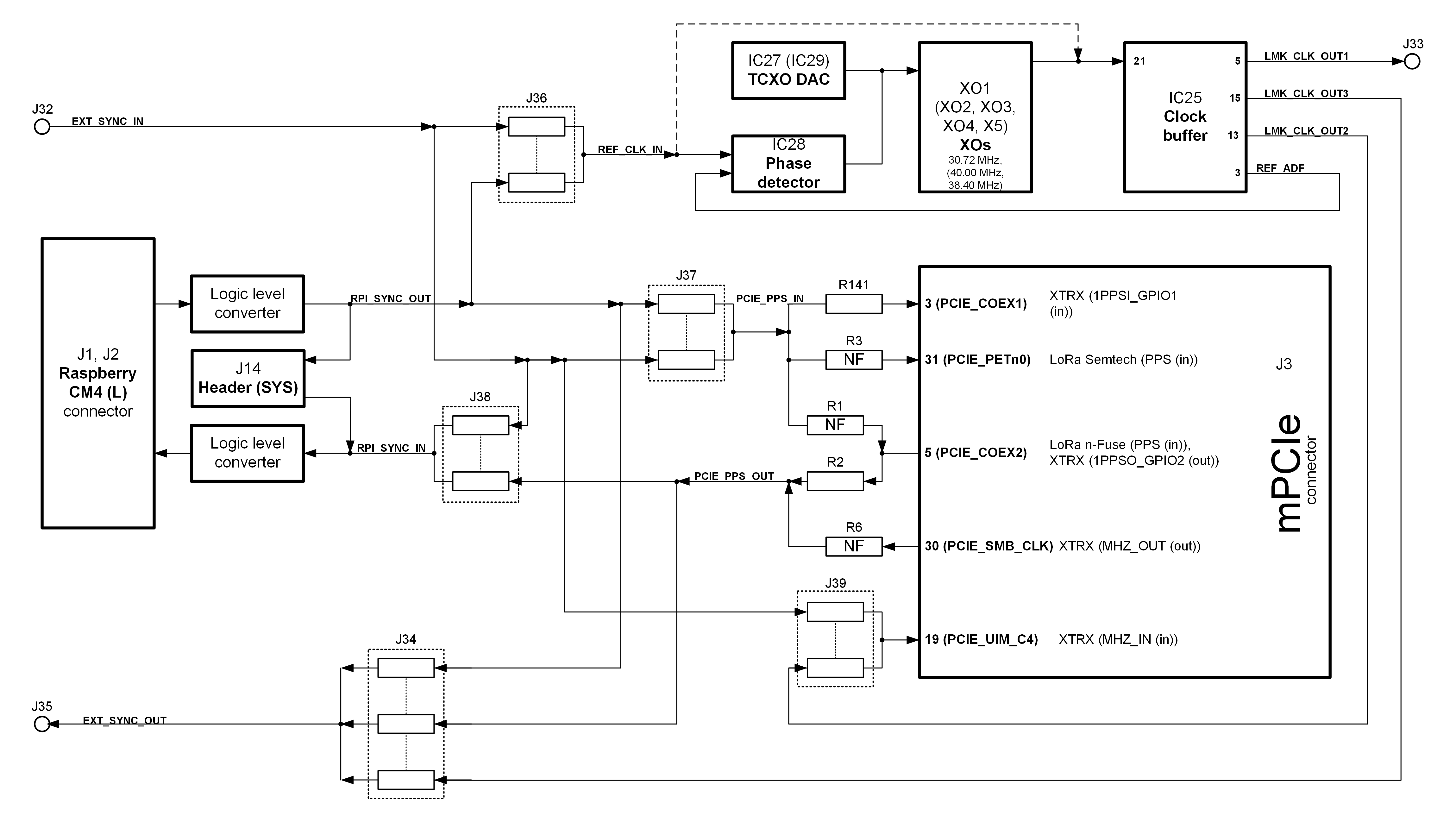
Figure 3. LimePSB RPCM 1v1 board clock distribution block diagram
LimePSB RPCM board distributes reference clock to and from Raspberry Pi Compute Module 4, mini PCIe connector and external sources. It is possible to connect external reference clock and PPS signals to and from another boards or systems via J32 (EXT_SYNC_IN) and J35 (EXT_SYNC_OUT) connectors. Clock path may be configured using jumpers and resistors as described in Table 17.
Schematic ID |
Input signal |
Output signal |
Description |
|---|---|---|---|
J36 |
EXT_SYNC_IN |
REF_CLK_IN |
Phase detector (IC28) input selection |
RPI_SYNC_OUT |
|||
J37 |
RPI_SYNC_OUT |
PCIE_PPS_IN |
PPS signal source selection for mPCIe expansion boards |
EXT_SYNC_IN |
|||
J38 |
EXT_SYNC_IN |
RPI_SYNC_IN |
CM4 SYNC_IN synchronization input source selection |
PCIE_PPS_OUT |
|||
J39 |
EXT_SYNC_IN |
PCIE_UIMC4 |
Reference clock selection for mPCIE exanpsion board (XTRX) |
LMK_CLK_OUT2 |
|||
J34 |
RPI_SYNC_OUT |
EXT_SYNC_OUT |
Synchronization output signal selection |
PCIE_PPS_OUT |
|||
LMK_CLK_OUT3 |
|||
R141 |
PCIE_PPS_IN |
PCIE_COEX1 |
PPS signal output for mPCIE expansion board (XTRX) |
R3 |
PCIE_PPS_IN |
PCIE_PETn0 |
PPS signal output for mPCIE expansion board (LoRa Semtech) |
R1 |
PCIE_PPS_IN |
PCIE_COEX2 |
PPS signal output for mPCIE expansion board (LoRa n-Fuse) and PPS output for (XTRX) |
R2 |
PCIE_COEX2 |
PCIE_PPS_OUT |
PPS signal input from mPCIE expansion board (XTRX) |
R6 |
PCIE_SMB_CLK |
PCIE_PPS_OUT |
Clock signal input from mPCIE expansion board (XTRX) |
LimePSB RPCM board has several on-board crystal oscillator (XO) options that may be used as source for clock buffer LMK00101. By default voltage controlled oven compensated crystal oscillator (VCOCXO) XO1 is populated. Optional voltage controlled temperature compensated crystal oscillators XO2 – XO5 (VCTCXO) are not populated by default. All these XOs may be tuned by DAC (16-bit IC27 default or 8-bit IC29) or phase detector (IC28).
Clock network components are listed in Table 18.
Designator |
Type |
Part number |
Description |
Description |
|---|---|---|---|---|
XO1 |
VCOCXO |
U7475LF 30.72MHz |
30.72 MHz |
|
XO2 |
VCTCXO |
E6245LF 30.72 MHz |
30.72 MHz |
Not mounted |
XO3 |
E5280LF 30.72MHz |
30.72 MHz |
Not mounted |
|
XO4 |
RTX5032A, 40.00MHz |
40 MHz |
Not mounted |
|
XO5 |
ASVTX-12-A-38.400MHZ-H10-T |
38.4 MHz |
Not mounted |
|
IC27 |
DAC |
AD5662 |
16 Bit |
|
IC29 |
AD5601BKSZ-REEL7 |
8 Bit |
Not mounted |
|
IC25 |
Clock buffer |
LMK00105SQ/NOPB |
||
IC28 |
Phase detector |
ADF4002BCPZ-RL7 |
Power Distribution
LimePSB RPCM board power delivery network consists of different power rails with different regulators, voltages and filters. LimePSB RPCM board power distribution block diagram is presented in Figure 4.
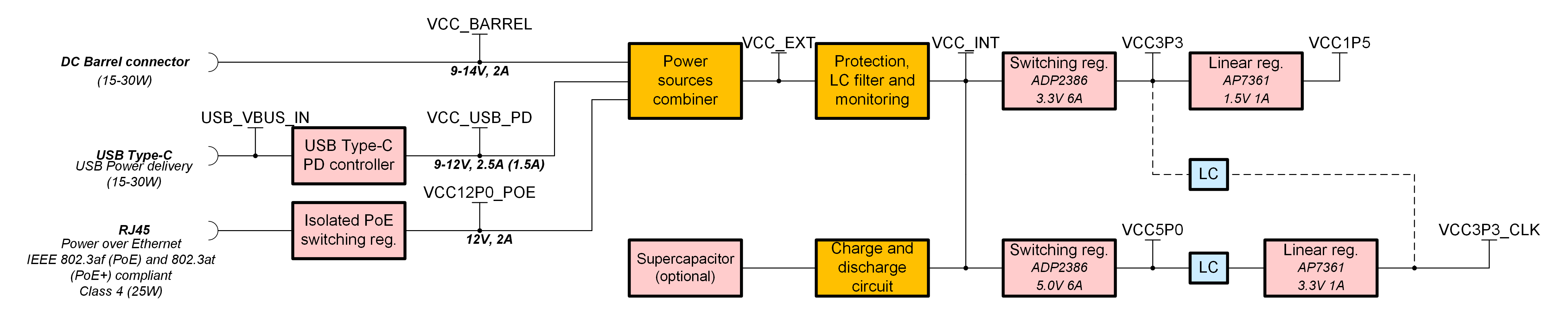
Figure 4. LimePSB RPCM 1v1 board power distribution block diagram
LimePSB RPCM board may be supplied from USB Type-C port (USB Power delivery), Ethernet RJ45 port (PoE) or barrel DC connector (9-14V):
USB Type-C socket (9-12V 2.5 A or 1.5 A) may be used to supply LimePSB-RPCM board. In this case make sure that USB Power Delivery 18W or more power adapter is used. Depending on application board requested current from source may be lowered from 2.5A to 1.5A by placing jumper on header J48.
RJ45 socket is an alternative way to supply the LimePSB RPCM board. Make sure PoE+ (802.3at) class 4 compliant power source is used.
Barrel connector (9-14V 2A) also may be used to power LimePSB RPCM board.
To keep RTC running when board power is disconnected 3V CR1220 battery must be inserted into BATT1 battery holder.